HDI (High-Density Interconnect) PCBs are designed to provide superior electrical performance. Their intricate layer structures and fine-pitch components significantly reduce signal loss and improve overall circuit performance. This makes them ideal for high-speed applications, where performance is critical.
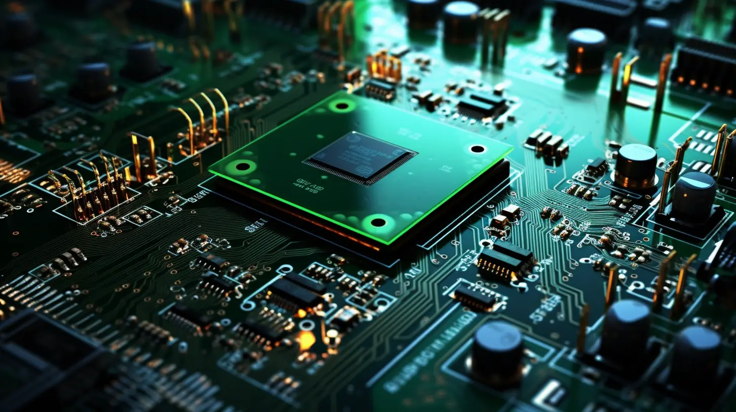
With the increasing demand for compact electronic devices, HDI PCBs offer a significant advantage. Their ability to accommodate more components in a smaller footprint helps manufacturers save valuable space, allowing for slimmer and lighter devices.
While HDI PCBs can initially seem more expensive, their enhanced functionality often leads to greater cost savings in the long run. The reduced number of layers and shorter interconnections can lower manufacturing costs and assembly time.
HDI PCBs are designed to manage heat more effectively than traditional PCBs. Their superior thermal conductivity helps dissipate heat efficiently, which is essential for high-performance electronics, ensuring reliability and longevity.
From smartphones to medical devices, HDI PCBs are versatile enough to be used in various high-tech applications. Their adaptability makes them suitable for a wide range of industries, which boosts their demand in the market.
In conclusion, choosing HDI PCBs for your projects can lead to remarkable benefits such as enhanced performance, space efficiency, cost-effectiveness, improved thermal management, and versatility across sectors. They are truly the backbone of modern electronic devices.


 55
|
55
|
 5G technology
high-speed PCB
telecommunications
5G technology
high-speed PCB
telecommunications
 30
|
Flexible PCB
High-frequency applications
Prototype boards
PI Polyimide
Low-loss dielectric
Electronics manufacturing
30
|
Flexible PCB
High-frequency applications
Prototype boards
PI Polyimide
Low-loss dielectric
Electronics manufacturing
 172
|
Precision engineering circuit board
Multilayer PCB
Flexible circuit board
287
|
Communication Network
High-speed PCB
IC Substrate
Data Center
Mingzhenghong Electronics
360
|
Consumer Electronics
smart phone
Laptop
Custom PCB
Multilayer IC substrate
172
|
Precision engineering circuit board
Multilayer PCB
Flexible circuit board
287
|
Communication Network
High-speed PCB
IC Substrate
Data Center
Mingzhenghong Electronics
360
|
Consumer Electronics
smart phone
Laptop
Custom PCB
Multilayer IC substrate