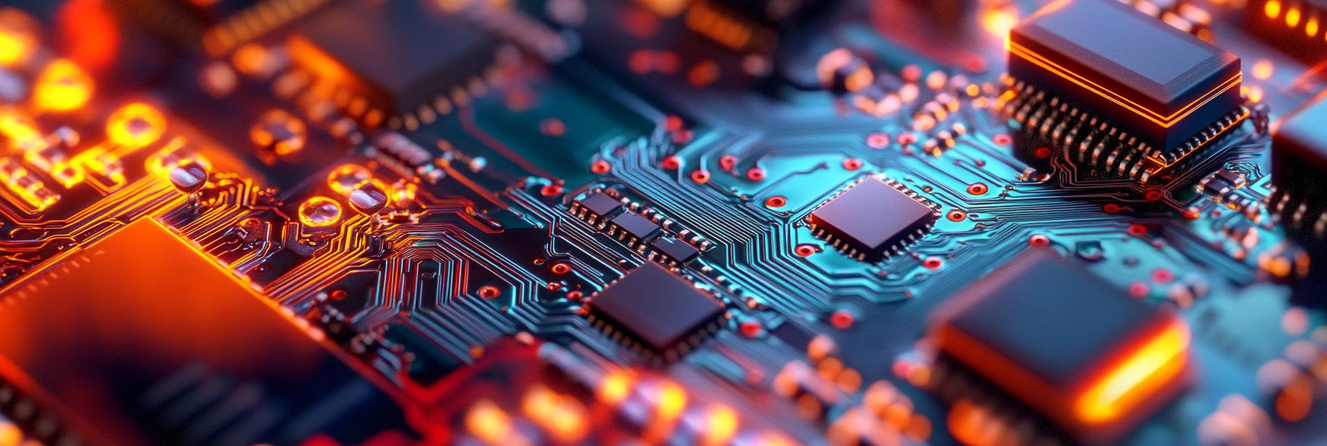
The advent of 5G technology has revolutionized the telecommunications landscape, paving the way for faster and more reliable communication. At the heart of this technology lies the high-frequency Printed Circuit Boards (PCBs), which are pivotal for the functionality of these advanced devices. This article will outline the complexities of the PCB manufacturing process, highlighting the materials and technologies that contribute to the performance of 5G communication devices.
High-frequency PCBs are designed to handle signals in the gigahertz range, making them essential for applications in 5G communication. Their design and manufacturing require precision and advanced materials to ensure minimal signal loss and maximum reliability.
The choice of materials is crucial in the production of high-frequency PCBs. Common materials include:
The manufacturing process begins with the design phase, where engineers create PCB layouts using advanced software. This includes considering factors such as trace width, layer stack-up, and material selection to optimize performance.
Once the design is complete, the substrate material is cut and treated to ensure compatibility with the etching and plating processes. This step is crucial for achieving the desired electrical properties.
This step involves applying a photoresist layer on the substrate, followed by exposing it to UV light through a photomask. The exposed areas are then developed, creating a protective pattern for the etching process.
With the photoresist in place, the bare copper is etched away from the unprotected areas, forming the conductive traces necessary for circuit functionality.
Post-etching, a plating process is employed to ensure the traces meet the required thickness, which helps in higher current applications and improves signal integrity.
The final step includes assembling components onto the PCB, followed by rigorous testing to ensure the board meets specified performance standards and operates effectively in 5G applications.
The manufacturing of high-frequency PCBs is a complex process that underpins the functionality of 5G communication devices. By leveraging advanced materials and innovative manufacturing techniques, manufacturers can produce PCBs that enhance the performance and reliability of modern telecommunications. As technology progresses, we can anticipate further advancements in PCB design and manufacturing that will continue to support the ever-evolving demands of the 5G landscape.

 455
|
455
|
 IC testing
high-density interconnect boards
HDI technology
printed circuit boards
PCB solutions
IC testing
high-density interconnect boards
HDI technology
printed circuit boards
PCB solutions
 216
|
Printed Circuit Boards
PCB manufacturing
electronic components
circuit design
PCB assembly
216
|
Printed Circuit Boards
PCB manufacturing
electronic components
circuit design
PCB assembly
 339
|
lead-free soldering
traditional soldering
soldering techniques
339
|
lead-free soldering
traditional soldering
soldering techniques
 435
|
multi-layer PCB
circuit boards
advanced PCB design
electronics manufacturing
435
|
multi-layer PCB
circuit boards
advanced PCB design
electronics manufacturing
 89
|
Precision IC Substrates
High-Speed PCB
Circuit Board Manufacturing
Multi-Layer PCB
89
|
Precision IC Substrates
High-Speed PCB
Circuit Board Manufacturing
Multi-Layer PCB


3.jpg?x-oss-process=image/resize,m_fill,h_300,w_300/format,webp)


