In today's fast-paced technological landscape, the demand for high-precision and reliable printed circuit boards (PCBs) has never been greater. Our High Precision Multi-Layer PCB Boards utilize advanced HDI technologies to deliver six-layer structures that meet the stringent requirements of various industries including telecommunications, medical, and industrial automation. This article will delve into the unique features and advantages of our HDI PCBs, showcasing their unparalleled performance and reliability.
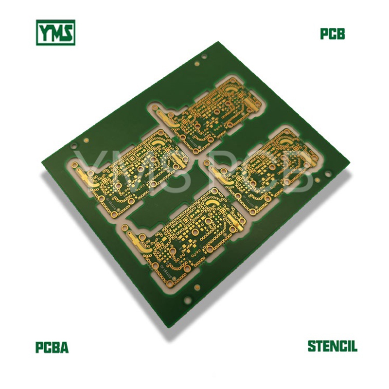
Our six-layer multi-layer PCB boards are meticulously designed with a board thickness of approximately 2.2mm and dimensions of 165mm x 110mm. We utilize 1 oz copper foil across both outer and inner layers in combination with FR-4 and ROGERS substrates, ensuring exceptional dielectric properties and thermal stability between layers. Additionally, our products feature minimal drill hole diameters of 0.2mm and a minimum line width/spacing of 4mil (0.1mm) to accommodate the highest precision requirements.
Our advanced multi-layer PCBs find applications in a variety of fields, such as:
In conclusion, our High Precision Multi-Layer PCB Boards offer advanced solutions for a range of critical applications, ensuring they meet the highest industry standards. With superior dielectric performance, stability, and reliability, they play a vital role in the ongoing evolution of technology across multiple sectors. For businesses looking to enhance their product offerings with top-tier PCB solutions, our HDI PCBs provide the ideal foundation for success.


 74
|
74
|
 PCBA stencil
SMT stencil
SMD stencil
frameless SMT stencil
high-precision PCB stencil
automated SMT stencil production
ISO certified SMT templates
environmentally friendly SMT stencil
customizable SMT templates
advanced PCB manufacturing solutions
PCBA stencil
SMT stencil
SMD stencil
frameless SMT stencil
high-precision PCB stencil
automated SMT stencil production
ISO certified SMT templates
environmentally friendly SMT stencil
customizable SMT templates
advanced PCB manufacturing solutions
 90
|
5G
High-Performance Circuit Boards
HDI
90
|
5G
High-Performance Circuit Boards
HDI
 441
|
Innovation Technology
Rapid Prototyping
High Precision
PCB
Electronics Manufacturing
441
|
Innovation Technology
Rapid Prototyping
High Precision
PCB
Electronics Manufacturing
 228
|
High Precision PCB
Six-layer structure
Electronic Applications
228
|
High Precision PCB
Six-layer structure
Electronic Applications
 275
|
High-density integration
High temperature resistance
Application Scenario
Core Technology
High reliability
275
|
High-density integration
High temperature resistance
Application Scenario
Core Technology
High reliability