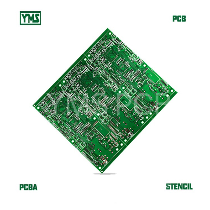
In the fast-paced world of electronics, achieving high precision in printed circuit boards (PCBs) is essential for ensuring optimal performance and reliability. The High Precision 34-Layer Laser Blind Hole PCB stands at the forefront of technological advancement, offering solutions tailored for demanding applications such as semiconductor testing, industrial automation, and high-density electronic integration. This article delves into the characteristics, advantages, and applications of this cutting-edge PCB technology.
The heart of the 34-layer PCB lies in its use of back-drilling and laser blind hole technologies. These innovations ensure that signal integrity is maintained across complex circuitry, which is crucial for precision applications. With a layer count of 34 and a maximum thickness of 5mm, this PCB can effectively support highly intricate circuit designs while providing stability and consistency.
The High Precision 34-Layer PCB is engineered to meet the stringent requirements of various sectors. Below are some notable applications:
In conclusion, the High Precision 34-Layer Laser Blind Hole PCB represents a pivotal advancement in PCB technology, characterized by its reliability and precision. Ideal for a broad spectrum of applications, this PCB not only meets but exceeds industry standards, making it a preferred choice for businesses seeking to enhance their electronic capabilities. Invest in quality connectivity and signal integrity with the high-performance PCB solutions designed by 明政宏电子有限公司.

 389
|
389
|
 High-Performance Flexible Circuit Boards
Automotive Electronics
Complex Environments
Reliability
Durability
High-Performance Flexible Circuit Boards
Automotive Electronics
Complex Environments
Reliability
Durability
 216
|
Printed Circuit Boards
PCB manufacturing
electronic components
circuit design
PCB assembly
216
|
Printed Circuit Boards
PCB manufacturing
electronic components
circuit design
PCB assembly
 209
|
High-Frequency PCB
Telecommunications Base Stations
High-Speed Circuit Boards
Telecom Infrastructure
RF PCB Technology
209
|
High-Frequency PCB
Telecommunications Base Stations
High-Speed Circuit Boards
Telecom Infrastructure
RF PCB Technology
 438
|
Precision engineering circuit board
High Precision PCB
FPC
automated industry
5G Technology
403
|
高TG PCB
Edge copper PCB
Multilayer printed circuit board
FR-4
Semiconductor Testing
438
|
Precision engineering circuit board
High Precision PCB
FPC
automated industry
5G Technology
403
|
高TG PCB
Edge copper PCB
Multilayer printed circuit board
FR-4
Semiconductor Testing


