High-density interconnect (HDI) printed circuit boards (PCBs) have revolutionized the semiconductor industry, providing solutions that meet the stringent demands of performance and reliability. In this article, we explore the advanced capabilities of our High TG IC Testing HDI PCB, highlighting its key features and applications in semiconductor testing.
As technology advances, the complexity of semiconductor devices increases, resulting in higher performance expectations. Tester platforms require PCBs that can withstand thermal stresses, deliver precise electrical performance, and support high-density interconnections. Manufacturers face the challenge of meeting these demands while ensuring reliability and efficiency in production.
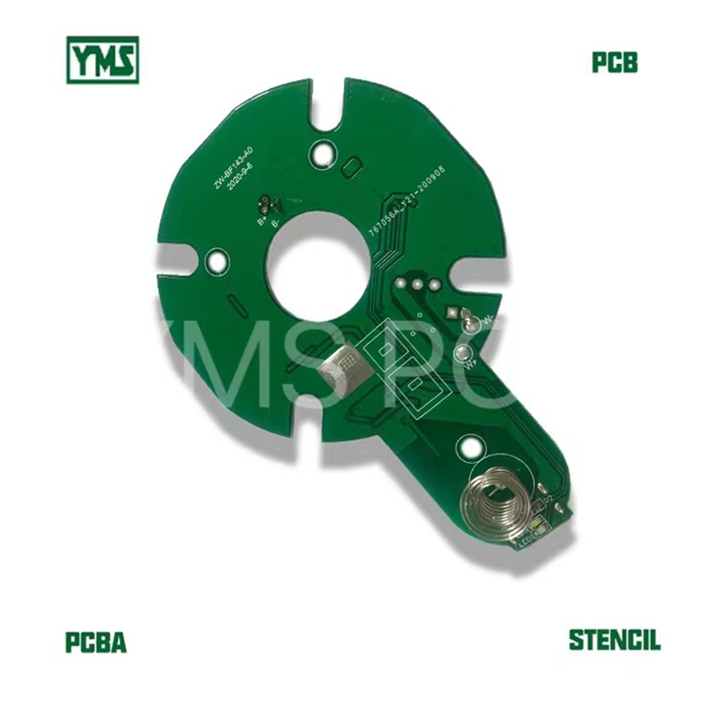
Our High TG IC Testing HDI PCB is engineered with high TG180 FR-4 material, which offers exceptional thermal stability and reliability under demanding conditions. With precise dimensions of 320X410mm (12.598X16.142 inches) and a thickness of 5.0mm, our PCB is designed to meet the rigorous requirements of semiconductor testing.
Our HDI PCB excels in various high-tech industries, including:
As the semiconductor industry continues to innovate, the demand for high-performance HDI PCBs like our High TG IC Testing solution will grow. By leveraging cutting-edge materials and technology, we provide manufacturers with the ability to meet these challenges with confidence, ensuring that their products remain at the forefront of the technology curve.
To learn more about our High TG IC Testing HDI PCBs and how they can enhance your semiconductor testing operations, view the image of our state-of-the-art PCB below:
Our commitment to quality and performance ensures that you get the utmost in reliability and efficiency for all your IC testing needs.


 370
|
370
|
 PCB certification
environmental PCB standards
sustainable electronics
eco-friendly PCB
PCB certification
environmental PCB standards
sustainable electronics
eco-friendly PCB
 431
|
medical device PCB design
PCB manufacturing trends
healthcare electronics
431
|
medical device PCB design
PCB manufacturing trends
healthcare electronics
 43
|
Flexible Printed Circuit Board
FPC
Digital Devices
43
|
Flexible Printed Circuit Board
FPC
Digital Devices
 260
|
Hybrid structure PCB
Four-layer rigid-flex PCB
High-performance PCB
Power Module
5G CPE equipment
Corrosion resistance
Electrical conductivity
260
|
Hybrid structure PCB
Four-layer rigid-flex PCB
High-performance PCB
Power Module
5G CPE equipment
Corrosion resistance
Electrical conductivity
 349
|
High Precision PCB
Circuit Board Assembly
Environmental certification
349
|
High Precision PCB
Circuit Board Assembly
Environmental certification


