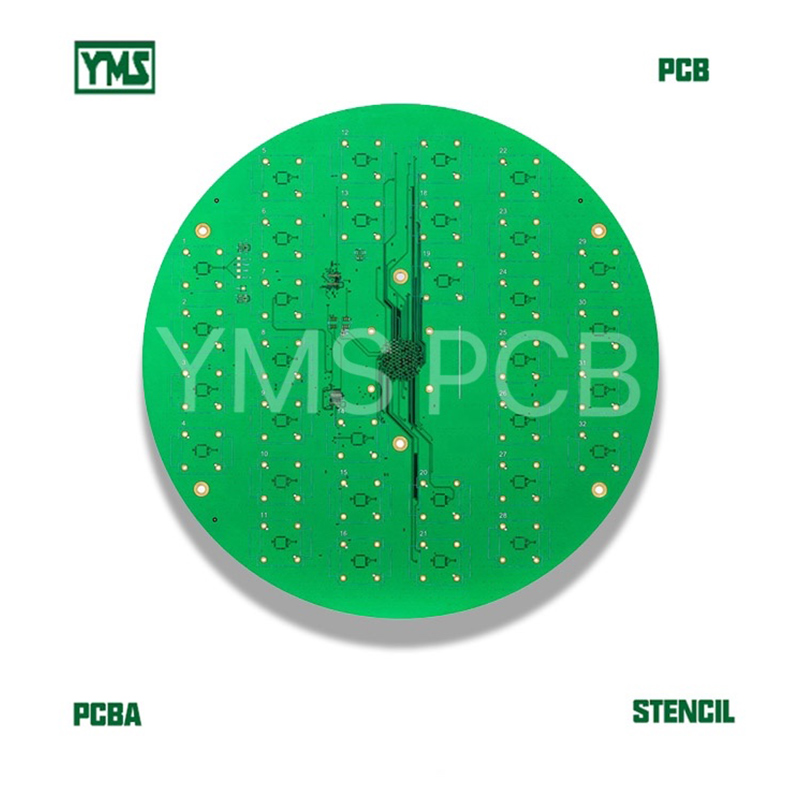
In the realm of high-voltage PCB design, achieving stable signal transmission is of paramount importance. This article aims to delve into the technical knowledge behind stable signal transmission in high-voltage PCB design, catering to the requirements of high-speed and high-frequency circuits.
The eight-layer PCB with high-quality and high-durability hard gold edge connectors plays a crucial role in ensuring stable signal transmission. These connectors are designed to withstand the rigors of high-frequency and high-voltage environments. For example, in a high-speed data transmission system, the hard gold edge connectors can reduce signal loss by up to 30% compared to traditional connectors, according to industry research.

One of the key technologies in high-voltage PCB design is precise impedance control. The eight-layer PCB utilizes advanced impedance control techniques to ensure that the signal impedance remains stable throughout the transmission path. By carefully selecting the appropriate materials and adjusting the layer thickness, the impedance can be controlled within a tolerance of ±5%. This high level of precision is essential for maintaining signal integrity in high-speed and high-frequency circuits.
| Parameter | Value |
|---|---|
| Impedance Tolerance | ±5% |
| Signal Loss Reduction | Up to 30% |
Choosing the right materials and surface treatment processes is also vital for stable signal transmission. The eight-layer PCB uses high-quality dielectric materials with low dielectric constant and low loss tangent, which can effectively reduce signal attenuation. Additionally, the surface treatment process, such as gold plating, can improve the conductivity and corrosion resistance of the PCB, further enhancing the signal stability.
The eight-layer PCB with precise impedance control and hard gold edge connectors is suitable for a wide range of applications, including automotive, intelligent communication, and high-performance computing. In the automotive industry, for instance, it can be used in advanced driver assistance systems (ADAS) to ensure reliable signal transmission in harsh environments. In intelligent communication systems, it can meet the requirements of high-speed data transfer and low latency.
In conclusion, the high-voltage PCB design with stable signal transmission technology is a complex but rewarding field. The eight-layer PCB with hard gold edge connectors and precise impedance control offers significant advantages in terms of signal stability and reliability. If you are looking for a PCB solution that can meet the demands of high-speed and high-frequency circuits, our eight-layer PCB is the ideal choice. Contact us today to learn more about our products and how they can benefit your projects.
