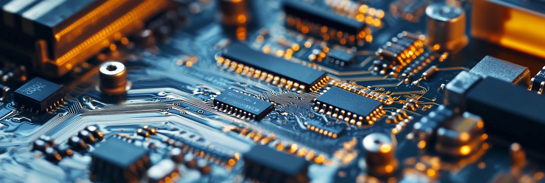
The field of high-frequency PCB circuit board technology has advanced rapidly, presenting both challenges and unprecedented opportunities for innovation. As the demand for more efficient electronic devices continues to grow, engineers and designers face complex hurdles that need to be overcome to meet these demands. This article delves deep into the current landscape, highlighting key issues and potential solutions.
One of the primary challenges in high-frequency PCB design is the use of materials that can withstand the increased thermal and electrical stress. Traditional materials often struggle to maintain signal integrity and are prone to issues such as dielectric losses. This necessitates a shift towards advanced materials that can support higher frequencies and reduce losses.
As frequencies increase, maintaining signal integrity becomes increasingly difficult. Issues such as crosstalk, reflections, and electromagnetic interference can severely impact performance. Engineers must adopt new design techniques that ensure minimal signal degradation while maximizing efficiency.
The fabrication of high-frequency PCBs often requires innovative manufacturing processes to meet stricter tolerances and more complex designs. Existing production techniques may not suffice, leading to delays and increased costs. This raises the need for the development of specialized manufacturing technologies capable of producing high-quality, reliable products.
Research into new high-frequency materials, such as low-loss dielectrics and advanced laminates, is essential. These materials should offer improved thermal stability, reduced losses, and overall enhanced performance. The integration of nanotechnology in material science also holds promise for revolutionizing PCB design.
To tackle signal integrity issues, designers can employ techniques such as impedance matching, careful trace routing, and power distribution network (PDN) design. Utilization of simulation software tailored for high-frequency applications can assist in predicting performance and optimizing designs before manufacturing.
The evolution of manufacturing technologies, including additive manufacturing and precision machining, can facilitate the production of complex PCB designs with greater material efficiency and accuracy. Collaboration between engineers and manufacturers will be critical in developing processes that meet the high standards required by the industry.
The challenges in high-frequency PCB circuit board technology are substantial, but they also pave the way for significant opportunities in innovation. By embracing advanced materials, innovative design techniques, and cutting-edge manufacturing processes, the industry can drive progress and shape the future of electronics. Staying ahead in this field requires adaptability, investment in R&D, and a commitment to continuous improvement.

 90
|
90
|
 Precision High TG IC Testing HDI PCB
High TG IC Testing PCB
Semiconductor Test HDI PCB
Precision High TG IC Testing HDI PCB
High TG IC Testing PCB
Semiconductor Test HDI PCB
 379
|
design process
production workflow
manufacturing optimization
379
|
design process
production workflow
manufacturing optimization
 73
|
medical devices
PCB design
product stability
73
|
medical devices
PCB design
product stability
 115
|
High-Power PCB
Impedance Controlled Circuit Board
Thick Copper PCB
FR-4 PCB
High Current PCB
115
|
High-Power PCB
Impedance Controlled Circuit Board
Thick Copper PCB
FR-4 PCB
High Current PCB
 449
|
Antenna Technology
Power Module
Four-layer rigid-flex PCB
449
|
Antenna Technology
Power Module
Four-layer rigid-flex PCB


